Since the beginning of semiconductor electronics in the 1940s and the development of transistors and solar cells, silicon has been leading the race for the best semiconductor of all time. The building blocks of modern computer chips are based largely on silicon, which is not surprising considering that silicon technology has been developed to perfection in the last years. Nevertheless, silicon is slowly reaching its limits. Compound semiconductors, composed of two or more elements, like for example gallium nitride (GaN), overcome silicon in speed, light detection and emission, and spin transport, which are expected to enable applications like 6G and self-driving cars.
What is a semiconductor?
As the name says, semiconductors are materials that can conduct a current, similar to metals. The advantage is, that in semiconductors the conduction can be tuned on demand during the fabrication. This is possible thanks to the so-called band gap – but what is this? The energy state of electrons (excited or at rest) can be described by the quantum mechanical band model. In semiconductors and insulators there is a gap in these energy bands. This means that there are certain energies, which are not allowed for electrons. One can picture this as a river: the electrons must cross this over, in order to get to the other shore and conduct a current. In metals there is not such a river, or energy gap.
In order to modify the conductivity of a semiconductor, one employs doping. This can be compared to a boat full with passengers (charge carriers). Charge carriers can be either electrons or holes, meaning empty spaces for the electrons. The more passengers on the boat, the easier these reach the shore and conduct currents. Doping of a semiconductor is achieved by adding foreign atoms.
Silicon and gallium nitride are semiconductors, which means, they can conduct current like a metal, but they can also be insulating.
GaN-based light emitting diodes
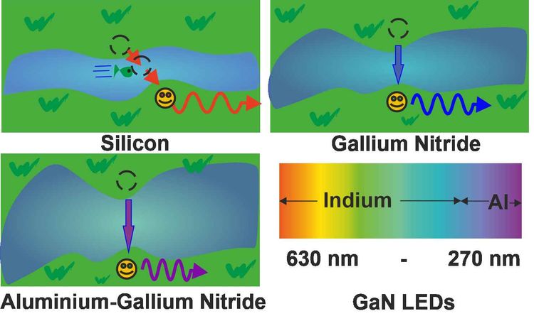
Semiconductors show an additional feature thanks to the band gap: they emit light. Electrons require energy to cross from the lower (valence band - at rest) to the upper (conduction band - excited state) shore of the river. However, due to the fact that electrons always prefer to be in the lowest energy state – just like us – they can cross over again into the valence band. Energy must be conserved. Therefore, while crossing back to the lower shore, the electrons release energy in form of an electromagnetic wave: it emits light. The color of the emitted light depends on how large the band gap is. Therefore, the width of the river dictates the wavelength of the emitted light.
Gallium nitride has a band gap of 3,4 electron volt (eV), which corresponds to a wavelength of 360 nanometers (nm; 0.00000036 m), meaning ultraviolet (UV) light. If we add Indium, then the band gap becomes smaller and the wavelength of the emitted light becomes larger, shifting the light emission from UV to blue and green. This is shown in the image above.
And here is where light emitting diodes (LEDs) come to play: a LED consists of the emitting semiconductor placed between two doped layers. An n-doped layer, meaning a layer with excess electrons, and a p-doped one, with an excess of missing electrons (or holes). By applying a current, the electrons and the holes meet at the emitting layer and recombine – this means the electrons fall into the free holes. The more electrons and holes are created by doping, the higher ist he probability that there will be emission. In 2014, Isamu Akasaki and Hiroschi Amano were awarded with the Nobel prize for physics for the invention of GaN-based the blue LED.
The band gap of GaN can be enlarged by adding aluminum. This allows making an LED in the deep UV (DUV). LEDs have a wide range of applications, due to the fact that they can be fabricated at low cost and are energy saving. DUV-LEDs can be employed for water purification, because light with a wavelength below 280 nm breaks the binding of organic molecules, leading to the deactivation of virus and bacteria. Through the addition of magnesium and manganese to GaN, emission in the infrared is achieved, allowing for GaN-based LEDs and lasers to be employed also in telecommunications.
Silicon has a very small band gap, still it cannot emit light easily. This is due to the fact, that the shortest transition across the river in silicon is not direct, meaning that electrons need additional help, like from a flying fish like in the image above, to reach to the other shore. Therefore, it is very difficult to make silicon emitt light.
Beyond light emission
Gallium nitride can do more than just emit light. It is robust and not poisonous, which allows employing this material into applications in different environments, ranging from space to medicine. Through the addition of transition metal atoms, like manganese and iron, GaN can become a magnetic semiconductor.
While manganese atoms can be homogenously diluted in GaN up to a concentration of 10%, iron atoms have a very small solubility limit, just like a lot of sugar in water. As a result, the iron atoms form together with the nitrogen tiny magnetic nanocrystals in GaN of 5 to 30 nm in size. The shape, size, crystal structure and number of these nanocrystals can be controlled on demand during fabrication, leading to different magnetic properties. The direction of the magnetic field inside these nanocrystals can be then switched through the application of an external magnetic field, opening potential applications in memory devices.
Last fall we demonstrated in the final of the Austrian Science Slam 2020 competition (see video above - only in German though), how versatile GaN can be and why it is for us definitely the allrounder among semiconductors.
Why has gallium nitride not beat silicon yet?
This is partly because GaN devices are fabricated mainly on sapphire substrates and sapphire is insulating. Moreover, the lattice constant – meaning the distance between two atoms in a crystal – of these two materials is very different, leading to the formation of defects. These defects are detrimental for the conduction of currents and light emission. Interestingly, GaN devices for high-power electronics are fabricated on silicon. This shows that, even if there might be an everlasting competition between these two materials for the best semiconductor of all times, they complement each other so well that they can be applied better together than individually.
On the other hand, GaN-based transistors can still not compete with silicon ones. However, this challenge has been researched extensively in recent years and it is only a matter of time before GaN also overcomes this hurdle. It is expected, that GaN in combination with superconductors like niobium nitride, or ultra-thin two-dimensional layers, lead to still unexplored and interesting applications and physics in the field of quantum materials. (Andrea Navarro-Quezada, Anna Spindlberger, 26.1.2021)
More blogposts